
The inductor is common energy storage passive component in the circuit, which plays the role of filtering, boosting, and bucking in the design of the switching power supply. In the early stage of solution design, the engineer should choose the appropriate inductance value. And consider the current that the inductance can withstand. If you are not familiar with the function of the inductor, you are often passive in the design and consume a lot of time.
Understanding the Function of Inductors
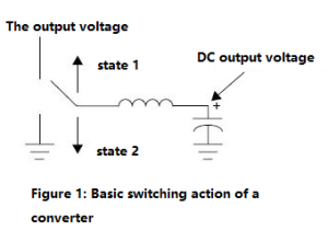
The inductor component is the “L” in the LC filter circuit at the output of the switching power supply. In step-down conversion, one end of the inductor is connected to the DC output voltage. The other end is connected to the input voltage or GND with switching frequency switching.
During state 1, the inductor is connected to the input voltage through the MOSFET. During state 2, the inductor is connected to GND.
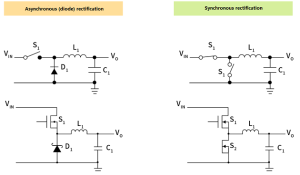
With this type of controller, the inductor can be grounded in two ways: through a diode or through a MOSFET. If it is the former way, the converter is called the asynchronous way. The latter method, the converter is called the synchronous method.
During state 1, one end of the inductor is connected to the input voltage and the other end is connected to the output voltage. For a buck converter, the input voltage must be higher than the output voltage, thus creating a forward voltage drop across the inductor.
During state 2, one end of the inductor originally connected to the input voltage is connected to ground. For a buck converter, the output voltage must be positive, thus creating a negative voltage drop across the inductor.
Inductor voltage calculation formula
V=L(dI/dt)
Therefore, when the voltage on the inductor is positive (state 1), the current on the inductor increases; when the voltage on the inductor is negative (state 2), the current on the inductor decreases. The current through the inductor is shown in Figure 2:
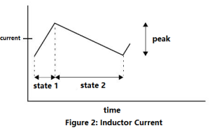
From the diagram above we can see that the maximum current flowing through the inductor is the DC current plus half of the switching peak-to-peak current. The graph above is also known as ripple current. According to the above formula, we can calculate the peak current: where, ton is the time of state 1, T is the switching period, and DC is the duty cycle of state 1.
Synchronous conversion circuit
![]()
Asynchronous conversion circuit
Rs is the sum of the inductive resistance impedance plus the inductive winding resistance. Vf is the forward voltage drop of the Schottky diode. R is Rs plus MOSFET on-resistance, R=Rs+Rm.
![]()
Saturation of Inductor Core
From the peak inductor current we have calculated, we know that as the current through the inductor increases, its inductance decays. This is due to the physical properties of the core material. How much the inductance decays is critical and important: if the inductance decays too much, the converter will not work properly. When the current through the inductor is so large that the inductor fails, the current at this time is called “saturation current”. This is also the basic parameter of the inductor.
It is very critical that the power inductor in the conversion circuit will have a saturation curve, which is worth noting. To understand this concept one can observe the curve of the actual measured LvsDC current:
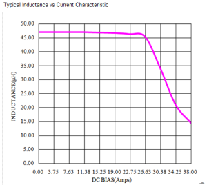
When the current increases to a certain level, the inductance will drop sharply, which is the saturation characteristic. If the current increases, the inductor will fail.
With this saturation characteristic, we can know why the inductance value variation range (△L≤20% or 30%) under the DC output current is specified in all converters, and why there is Isat in the inductance specification parameters. Since the ripple current changes will not seriously affect the inductance. In all applications, it is desirable to keep the ripple current as small as possible because it affects the output voltage ripple. This is why people are always concerned about the attenuation of the inductance under the DC output current, but ignore the inductance under the ripple current in the specification.
Choosing the Right Inductor for Switching Power Supplies
The inductor is a commonly used component in switching power supply because its current and voltage phase is different, so theoretically the loss is zero. Inductors are often energy storage components, which have the characteristics of “rejecting and staying”. They are often used in input filtering and output filtering circuits together with capacitors to smooth the current.
Inductors are magnetic components and naturally have the problem of magnetic saturation. Some applications allow the inductor to saturate, some allow the inductor to enter saturation from a certain current value, and some do not allow the inductor to saturate, which requires distinction in specific circuits. In most cases, the inductance works in the “linear region”, in which the inductance value is constant and does not change with the terminal voltage and current.
However, there is a problem we cannot ignore in the switching power supply, that is, the winding of the inductance will lead to two distributed parameters (or parasitic parameters), one is the inevitable winding resistance, and the other is the distribution related to the winding process and material. stray capacitance. Stray capacitance has little effect at low frequencies but gradually becomes apparent as the frequency increases. When the frequency is higher than a certain value, the inductance may become a capacitive characteristic. If the stray capacitance is “concentrated” into one capacitance, the capacitance characteristic after a certain frequency can be seen from the equivalent circuit of the inductance.
Job Features
When analyzing the working condition of the inductor in the circuit, the following characteristics must be considered:
- When a current I flows through the inductor L, the energy stored in the inductor is: E=0.5×L×I2(1)
- In a switching cycle, the relationship between the change of the inductor current (the peak-to-peak value of the ripple current) and the voltage across the inductor is: V=(L×di)/dt(2).
- The inductor also has the process of charging and discharging voltage. The current across the inductor is proportional to the integral of the voltage (volts per second). As long as the inductor voltage changes, the current rate of change di/dt will also change; the forward voltage causes the current to rise linearly, and the reverse voltage causes the current to drop linearly.
Inductor selection of step-down switching power supply
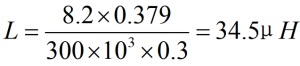
When selecting an inductor for a step-down switching power supply, it is necessary to determine the maximum input voltage, output voltage, power switching frequency, maximum ripple current, and duty cycle. The below diagram describes the calculation of the inductance value of the step-down switching power supply. First, it is assumed that the switching frequency is 300kHz. The input voltage range is 12V±10%, the output current is 1A, and the maximum ripple current is 300mA.
Circuit diagram of step-down switching power supply
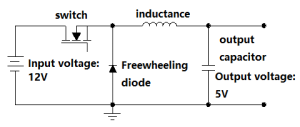
The maximum input voltage value is 13.2V, and the corresponding duty cycle is:
D=Vo/Vi=5/13.2=0.379(3)
Among them, Vo is the output voltage, and Vi is the output voltage. When we turn on the rocker switch, the voltage on the inductor is V=Vi=5.5V (8).
V=Vi-Vo=8.2V(4)
When we turn off the switch, the voltage across the inductor is:
V=-Vo-Vd=-5.3V(5)
dt=D/F(6)
Substituting Equation 2/3/6 into Equation 2 gives:
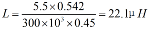
Inductor Selection of Boost Switching Power Supply
The calculation of the inductance value of the step-up switching power supply is the same as that of the step-down switching power supply, except that we change the relationship between the duty cycle and the inductor voltage. Assuming that the switching frequency is 300kHz, the input voltage range is 5V±10%. And the output current is 500mA, the efficiency is 80%. The maximum ripple current is 450mA, and the corresponding duty cycle is: D=1-Vi/Vo=1-5.5 /12=0.542(7)
Circuit diagram of the boost switching power supply
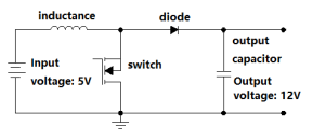
When we turn on the rocker switch, the voltage on the inductor is V=Vi=5.5V (8). When the switch is off, the voltage on the inductor is: V=Vo+Vd-Vi=6.8V (9) Put the formula Substituting 6/7/8 into Equation 2 yields:
Note that a boost power supply differs from a buck power supply in that inductor current does not always provide the load current. When we turn on the switch, the inductor current flows into the ground through the switch, and the output capacitor provides the load current. But when we turn off the switch, the current flowing through the inductor provides the load and charges the output capacitor.
Generally speaking, the larger the inductance value is, the smaller the output ripple will be. But the dynamic response of the power supply will also be correspondingly worse. So we can adjust the selection of the inductance value according to the specific application requirements of the circuit. The increase of the switching frequency can make the inductance value smaller. Thereby reducing the physical size of the inductance and saving the space of the circuit board. Therefore, the current switching power supply has a trend of high-frequency development. In order to meet the requirements of smaller and smaller electronic products.
Analysis and Application of Switching Power Supply
Lenz’s law-related content: When we use the DC power supply, due to the self-inductance of the coil, the coil will generate a self-inductive electromotive force. This will hinder the increase of the coil current, so, at the moment of power-on, we can consider the circuit current to be 0. At this time, all the voltage drop of the circuit falls on the coil, then the current increases slowly, the voltage at the coil terminal drops slowly until zero, and the transient process ends.
During the switching operation of the converter, we must ensure that the inductor is not in saturation. The saturable inductance is equivalent to a straight-through DC path in the circuit, so it cannot store energy. And it will defeat the entire design of the switch-mode converter. When we determine the switching frequency, the inductance working with it must be large enough.
We determine the inductance in the switching power supply: the switching frequency is low, and the on and off times are relatively long. So to keep the output uninterrupted. We need to increase the inductance value. So that the inductance can store more magnetic field energy. At the same time, because each switch is relatively long, the supplementary update of energy is not as timely as when the frequency is high, so the current will be relatively small. This formula can illustrate the principle:
L=(dt/di)*uL
D=Vo/Vi, buck duty cycle D=1-Vi/Vo, boost duty cycle
dt=D/F, F=switching frequency
di = current ripple
Therefore, L=D*uL/(F*di), when the switching frequency of F is low, L needs to be larger; we agreed that when we set L to large, the ripple current di will relatively reduce. At high switching frequencies, increasing the inductance will increase the impedance of the inductance, increase power loss, and reduce efficiency. But the dynamic response of the power supply will also correspond accordingly. Therefore, we can adjust the selection of the inductance value according to the specific application requirements of the circuit.